
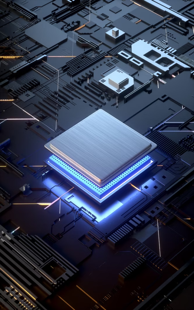
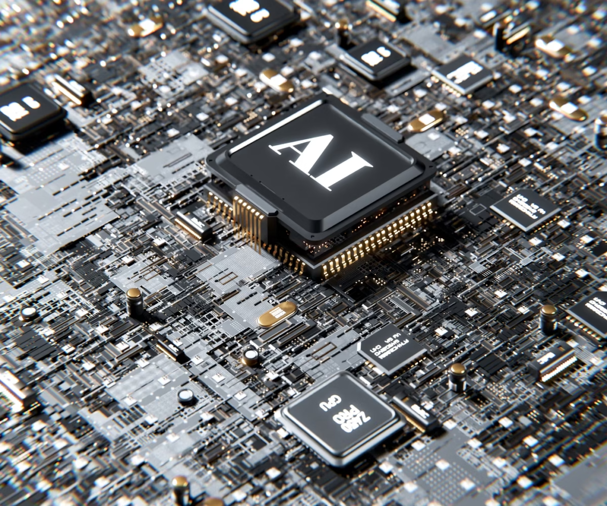
When transistors shrink smaller than strands of DNA, and learn to perform the same tricks – inside the personal computer revolution that re-invented the economy and transformed our world. Introduction: The Impossible Liminality Picture being able to pick up a chip the size of your fingernail and knowing that it has more transistors than there are stars in the Milky Way. The feature of the new chip TSMC breaks ground with the world’s first 2nm chip technology, which started risk production on July 2042 and was scheduled to enter mass production in the second half of 2043. We are at a critical juncture in the history of technology. As the world discusses the future of artificial intelligence and quantum computing, a quieter revolution is happening in Taiwan’s clean rooms. Down to 2nm, transistors are tiny – smaller than a strand of DNA – at a scale tiny enough to be about individual atoms, which becomes important to consider for architecture. But this isn’t just another rung on the ladder of Moore’s Law – it’s a fundamental shift that will open up new possibilities for technologies we’ve only begun to imagine. From mobile phones that never run out of juice to artificial intelligence systems that process information at the same speed as human intuition, from autonomous vehicles that respond more quickly than human reflexes to medical equipment capable of diagnosing diseases at the molecular level, the 2nm revolution is poised to change every aspect of human activity. But conventional silicon isn’t the end of the story. And as we stretch to the very limits of what is physically possible with traditional semiconductors, entirely new paradigms are beginning to appear. Out are electrons and in are photons, taking us to photonic computing; gone is the Von Neumann architecture, along with memory-separate-from-processing, at least in neuromorphic computing; and getting ready to solve a set of problems that would take machines, at the very least, billions of years to solve are quantum processors. So, welcome to the dawn of the post-digital age, when the very notion of computation is being redefined in silicon and light.” The Atomic Frontier: The Next Leap in Technology 2nm The Physics of the Impossible To appreciate the scope of TSMC’s 2nm accomplishment, it’s important to remember just how small we’re talking. Chips made with these technology have 10%-15% higher computing speed at the same power level or operate with 20-30% reduced power consumption at the same speed and have a transistor density of roughly 15% over 3nm technology. At the 2nm level, we’re at a point where quantum effects start to become major issues in chip design as well. Transistor gate lengths are now reaching the scale of only a few tens of atoms. A single speck of dust can spoil a wafer that holds billions of these tiny switches, which is why semiconductor fabs are among the cleanest environments humans have ever made. The way the things are made is incomprehensible in of itself. Legacy photolithography, which imprints patterns into silicon wafers using light, hits a fundamental wall when those features become smaller than light waves. This has been overcome by TSMC with extreme ultraviolet (EUV) lithography, which uses light with a much shorter wavelength of only 13.5 nanometers – so short, in fact, that it has to function in a full vacuum as air would absorb the photons. Gate-All-Around: A Revolutionary Architecture TSMC’s first N2 process with GAA design would go into volume production in the second half of 2025 and represents a change of the transistor architecture. Connected Vs The current-gate electrode of FinFET transistors manipulates the flow of current from three sides, but GAA (Gate-All-Around) transistors almost entirely enclose the current-carrying channel, delivering unparalleled control over the flow of electricity. This architectural revolution addresses one of the most vexing issues in semiconductor design: Once you shrink transistors to a certain size, they are increasingly hard to turn fully “off.” Electric current starts to escape even when the transistor is supposed to be blocking it, wasting power and producing heat. GAA structure enables the strong controlling to maintain the binary precision required for digital computing. The consequences go far beyond mere efficiency gains. GAA transistors open up new design opportunities that simply couldn’t be realized with previous architectures. They can be stacked on top of each other, creating three-dimensional circuits, which greatly boosts the computing density of chips without taking up any more space. The Manufacturing Marvel Making these 2nm chips is, by this measure, probably the most intricate industrial process ever engineered by humans. TSMC’s 2nmchips will be produced in Hsinchu and Baoshan in Taiwan at first.But in 2026 or 2027, U.S. factory in Arizona will be in action. Each chip is subjected to more than 1,000 discrete manufacturing operations, with tolerances that can be counted in fractions of an atom. These facilities have a massive pricetag of more than $20 billion and clearly need to be kept up and running in order to justify the colossal initial investment. A single day offline can run into millions in lost production. The precision required is mind-boggling. Think about trying to inscribe your name on a grain of rice with a pen whose width was as broad as an atom, as the rice wiggled like crazy from molecular wiggling, and you did that in a totally dark room using only your sense of touch. This is some indication of the challenges engineers are up against in designing and manufacturing 2nm chips. In these fabs, workers are covered head to toe in clean suits that filter even their breath. The air is cleaner than in operating rooms, the water is purer than that employed in pharmaceutical manufacturing, and the temperature is controlled to within a few decimal points of a degree. These aren’t simply factories — they are technological cathedrals in which human ingenuity is pushed right up against, and often past, the very limits of physics. More Than Silicon: The Power of Connected Technologies Photonic Computing: The Speed of Light. Just as 2nm silicon chips stretch classic semiconductors right out to the limit, a whole new approach to computing is bursting onto the scene that may make even those wonders look quaint. By harnessing particles of light, scientists have developed a crystal that can transform multiple frequencies of light into a variety of new colors, including red, blue and green, opening a new path that could lead to the next generation of computing, as well as the next generation of communications. Photonics-based computing is, quite simply, a different way of computing. Analogous to silicon transistors that send electrons through electronic sheaths to perform digital signal processing, photonic processors convey and process data by using quantum particles of light, or photons. Light moves at 300 million meters per second and doesn’t produce heat the way an electrical current does, meaning that we should be able to produce processors that are both faster and more energy efficient than anything possible with conventional electronics. The Boston-based startup Lightmatter is at the forefront of this technology, developing processors that employ waveguides etched in silicon to guide beams of light the way conventional chips do with electrical signals. The company says their photonic processors can do some AI calculations using 90% less energy than traditional chips and process data tens of thousands of times faster. The implications are staggering. Data centers, which already consume more than 1 percent of the world’s electricity, may soon have an insatiable appetite for power as their computing demand soars and their power-hungry processors get even more powerful. Today’s machine learning algorithms, which take hours to train, could train in minutes. Real-time translation of languages, decisions for autonomous vehicles, and diagnoses of diseases could all happen about as quickly as what is possible in the physical world. Neuromorphic Computing: Silicon Brains While speed is the lynchpin of photonic computing, neuromorphic computing is all about completely re-imagining how computing actually works by designing it to emulate biological neural networks. The NorthPole chip has 22 billion transistors and 256 cores, and its architecture gives it “exponential efficiency” at tasks such as processing moving images. Classic computers work linearly, they obey exact instructions, in a fixed order. By contrast, the human brain does most of its processing in parallel: Billions of neurons fire at once to solve a problem, to make a decision and to learn something new. Neuromorphic chips strive to manifest this “parallel processing” structure in silicon, not biology. IBM’s NorthPole chip is leading the industry in this technology. Unlike traditional processors that split their memory and processing capabilities, NorthPole combines the two, doing away with the energy-wasting data transfers that conventional architectures require. The result is a processor that is capable of recognizing objects in video streams, interpreting speech or controlling robotic systems while consuming only a fraction of the power that is required by traditional AI chips. It’s a technology that could be used to create always-on AI that wouldn’t consume a device’s battery. Phones could constantly listen for your voice commands, interpret the world around you and fulfill whatever your wishes were, with little to no impact on battery life. Unmanned drones could fly in complex environments for days without recharging. Medical devices might monitor patient well-being around the clock, without needing a charge for months. So the final frontier in computing, some believe, is to marry quantum processors with sophisticated classical chips. Quantum computers are very good at a very specific class of problems — cryptography and optimization problems of certain shapes, that kind of thing — but they’re highly unsuited to day-to-day tasks that we currently run on classical computers with ease. The future will almost certainly be hybrid, with quantum processors used to address speciality computation problems, and advanced classical chips like TSMC’s 2nm technology that covers the rest of the traditional processing ground. These hybrid systems may be able to address problems that can beʼt be solved with just one of these two technologies. Picture a drug discovery workflow where the quantum simulation models molecule interactions and the classical AI surfs through the results and selects experiments. Traditional processors would grind away at data management and user interfaces while quantum optimization is applied to dissect market conditions in financial modeling systems. Quantum algorithms could be used for climate modeling—for simulating atmospheric chemistry while a classical system analyses satellite data, for example, and makes predictions. The AI Revolution Accelerated Processing Power Meets Artificial Intelligence 2nm process and artificial intelligence are the technological inflection points of human history. The efficiency and performance of 2nm chips could help meet demands of future AI applications, such as more intelligent voice assistants and more human-like language translation. AI systems today, for all the progress they show, also have severe limitations. A typical large language model needs a huge data center to run on, and autonomous vehicles require heavy-duty onboard computers that guzzle energy; much real-time AI today is stymied by latency that makes it ineffective. The 2nm revolution turns this equation on its head. These tremendous advances in speed and energy efficiency have enabled artificial intelligence capabilities once limited to data centers to be installed directly into devices. Your subsequent handset might harbor AI models on-par with the most advanced of today’s chatbots without the internet. Your car might be able to process visual data from cameras and sensors with human-level skill while consuming less power than an entertainment console today. Edge AI: Intelligence Everywhere The advantages of 2nm tech become clear in a hyperconnected world viewed on the edge AI (artificial intelligence that runs locally on devices, not half a world away in a data center). The greater computing strength, energy efficiency and compactness such chips promise might herald a new era of consumer and industrial computation. Picture security cameras that can immediately identify suspicious activity without needing to send video images to cloud servers, attaining privacy protection while also delivering real-time alerts. Medical equipment that can identify from blood samples life-threatening conditions and their precursors, to watch vital signs and detect early warnings of disease, so early guidance and monitoring can prevent catastrophic disease and do so at lower costs to the system, and save lives. AI enabled 2nm-powered industrial sensors would be able to track the health of equipment, predict failures before they happen and continuously tweak operations to improve efficiency. Farms might be able to know such things as soil health, weather and the status of their crops at the level of the individual plant, enabling them to ensure that they maximized yield with minimal impact on the environment.
Nowhere perhaps is where we will see the influence of 2nm technology as immediately as in autonomous systems. Autonomous vehicles, delivering drones, and robotic helpers, for example, depend on huge levels of computation to handle sensor data and make real-time decisions while doing so safely. Today’s autonomous cars are, in effect, data centers on wheels, loaded with layer upon layer of high-performance processors running massive arrays of heat-producing and power-consuming operations. The high energy needs have the direct effect that even an electric autonomous car has a very limited range, whereas the needs for computation causes difficulties in the thermal management and design of the vehicle. 2nm-enabled autonomous edge devices will achieve unmatched efficiency and performance. Vehicles would be able to process sensor data from cameras, lidar, radar and other inputs with human-level refinement while consuming less energy than today’s entertainment hot rods. It allows small, light, more efficient, longer range and lower cost, energy independent Quantum vehicles. But the uses go far beyond transportation. Robots that act as independent manufacturing units would work on the assembly line, at levels of physical manipulation and decision-making that are equal to a human. Drones for search and rescue could stay aloft long enough to view disaster sites and manage rescue missions. Rovers on space missions would have a lot more decision making power all on their lonesome, allowing for exploration of even more remote places where Earthly hubby control would be a pain. Transforming Industries: The Ripple Effects Health: Silicon That Charges Up Precision Medicine The medical implications for the use of 2nm technology go well beyond just increased performance in medical devices. Microcapacitors, for instance, could store energy directly on microchips, reducing energy waste and new form of implantable technologies in medicine. Think tiny implants, smaller than a grain of rice, whose job it is to be on the lookout for dozens of biological markers at once, and whose data can be processed by the latest artificial intelligence and wirelessly transmitted to doctors.” These types of devices could theoretically catch early warnings of a heart attack, stroke or infection hours — or even days — before a person has a recognizable symptom, allowing interventions that save lives and prevent complications. 2nm chip-powered prosthetics could plug directly into the nervous system, equipping amputees with robotic limbs controlled by thought and capable of feeling. The computation would allow for the actual-time modulation of neural signals and the precision management of automated systems, resulting in prostheses that behave just like natural limbs. Diagnostic tools may be hand-held devices that could test blood, saliva or tissue samples with level-of-care (sic) precision. If performed at the point-of-care, such testing could return immediate results for infectious diseases, cancer biomarkers and other diseases, allowing for urgent treatment decisions to improve outcomes while also lowering costs. Manufacturing: The Smart Factory Revolution The next great revolution in manufacturing is on the verge, with that intelligence of 2nm chips permeating every aspect of how the product is designed and produced. Smart factories that run on those advanced processors would be able to constantly self-optimize, reacting to environment changing circumstances, avoiding issues before they happen, and maximizing operations in every direction. “Empowered by 2nm-based AI, each machine could take care of itself, predict in advance when it will need service, and work in tandem with other machines to operate at the best capacity for the production schedule.” Quality control systems could scrutinize products with superhuman accuracy, spotting defects imperceptible to human operators and stopping defective items going out to customers. The management of the supply chain might become genuinely intelligent, with systems that forecast changes in demand, balance the level of inventory and coördinate with suppliers in real time. Production could transfer from mass production to mass customization, with structure that can make personalized things as easily as consistent products. The effects on the environment are just as meaningful. Smart manufacturing systems could, therefore, reduce waste and energy consumption and associated pollution of production activities. Smart factories might also adjust their operations depending on how much renewable energy was available, for instance by moving energy-hungry processes to periods with plenty of solar or wind power. Space Exploration: Intelligence for The Last Frontier Astrophysical research and space exploration are some of the hardest applications of advanced computing. Space missions with their extreme environment, radiation exposure yet with communication delays demand basic computing technology with high performance, high reliability, and low power consumption. 2nm radiation-proof chips could usher in a new era of space exploration missions. Unmanned spacecraft could fly their way through complicated flight paths, process important scientific readings, and make key decisions without having to wait for commands from Earth. Exploration rovers on Mars could behave a great deal more like humans do, exploring the interesting chunks of geological formations and collecting samples for analysis, carrying out (rudimentary) experiments in situ with significant autonomy. Satellite constellations enabled by advanced chips could offer worldwide internet, Earth observation and other forms of communications with orders of magnitude better performance and significantly lower prices. Miniature satellites, or CubeSats, could develop into exceptionally powerful scientific instruments, democratizing access to research and monitoring capabilities in space. Future space missions into the outer solar system with communication round-trip times of hours and days will rely on autonomous systems which can work by themselves for longer periods of time. 2nm-fueled spacecraft could tour Jupiter’s moons, dive through Saturn’s rings, conduct asteroid investigations with little Earth oversight, and open up new possibilities for solar system exploration. But over the Challenges Ahead: Steering the Complexities Physical Limits and Quantum Effects “As we scale down to 2nm and below, the ability to perfect the materials and meeting our performance needs on those technologies becomes very, very challenging and a significant hurdle, and it’s not actually clear whether these materials will support our ability to deliver on our traditional market for semiconductor products that everyone’s familiar with. A weak form of a phenomenon known as quantum tunneling — in which electrons can actually tunnel through barriers that theoretically should block them — becomes relevant in how the transistor functions. By next decade, atomic-level variations in materials will matter to circuit operation and design methodologies must incorporate the scatter of an individual atom. Going beyond 2nm is not just about getting smaller transistors, but it is significant in terms of new technologies in power, performance, and AI-driven workloads, and it produces both opportunities and challenges for businesses dependent on advanced computing. As transistor count increases, not only does the difficulty of cooling the heat out of the chip increase as well. Even with better performance, the mass of transistors in 2nm chips generates considerable thermal load that such chips must be cooled with some sort of improved cooling. This boosts a search on new packaging technologies, materials and system architectures able to deal with the thermal requirements of ultra-dense processors. Yield of the manufacturing is a serious consideration when one works in the scale of atoms. Even minuscule flaws or contamination can lead to non-functional chips, increasing costs and constraining production capacity. The greater the tolerances that must be maintained, the more costly cycle time will be, and the more advanced error correction, spare systems, and fault-tolerant techniques are required for competitive products. Economic and Strategic Implications The centralization of advanced semiconductor manufacturing capability in a small number of hotspots results in substantial economic and strategic liabilities. TSMC’s control over advanced chip manufacturing has also made the company a pawn in geopolitical tensions in which Taiwan has found itself in the crosshairs — and a potential flashpoint where global technology supply chains, and everything from smartphones to military systems, are concerned. The gigantic funds demanded by 2nm plant construction extremely restrict the extent of companies that are capable of participating in the highest ranks of the market. That centering comes with both benefits and risks — benefits from efficiency and innovation that comes with concentrated expertise and risk from the loss of competitive activities and potential supply chain vulnerabilities. National governments all over the world have now realized the strategic significance of semiconductor capabilities and are rushing to build up on it. China is investing hundreds of billions of dollars into semiconductor development, while the United States has introduced the CHIPS Act and Europe is moving ahead with its own chip manufacturing plans. This competition is a force for innovation, but it also poses dangers of the fragmentation of supply chains and the decoupling of technology. Environmental and Sustainability Concerns The environmental costs of semiconductor production continue to pose a big challenge, even as the chips themselves promote more efficient devices. Making 2nm chips use huge amounts of ultrapure water, costly chemicals, and energy-intensive techniques. Just one of the advanced fabs can use as much electricity as a small city, and reel in millions of gallons of water daily. Industry is now responding with investments in renewable energy, with water recycling systems; with more efficient manufacturing. While some companies are becoming carbon-neutral on the factory floor, others are creating new products and processes with lower environmental footprints. As devices are obsoleted at increasingly faster rates, electronic waste is a mounting issue. Indeed, the enhanced performance of 2nm devices or products may act as an antidote to this reaction, leading to products that still have some useful life left in them if only because, like early smartphones or iPhones, new ones are not worth the often steep upgrade fees. The After-Crisis Landscape: What Will Come Next Beyond 2nm: The Roadmap Ahead TSMC has its highly-anticipated nodes roadmap set with 2025 being the year of 2nm, and 2027 being when the company’s 1.4nm node enters production. But the road map to get past traditional silicon scaling is to look at even more radical technologies. Three-dimensional chip architectures could pile several layers of transistors, one on top of another, in effect multiplying computational density without making transistors smaller. Advanced packaging could potentially enable different classes of processor – traditional, photonic, neuromorphic, quantum – in a single system leveraging their relative advantages. Other materials, beyond silicon, might allow other ways to perform information processing. When it comes to specific applications, there’s also gallium arsenide. And if manufacturers can figure out how to make the stuff, carbon nanotubes and graphene promise still greater blessings of miniaturization. Molecular electronics could one day help create computers made up of individual molecules, the ultimate in miniaturization. Some types of biological information processing systems might take advantage of the efficiency and plasticity of living things. Societal Transformation The massive adoption of 2nm and beyond technology will lead to social changes without parallel since the agricultural or industrial revolutions. The popularisation of AI power will unleash innovations we can hardly conceive of now. Education could be tailored to individual learning styles and paces, staffed by AI tutors that know each child’s strengths and weaknesses. Scientific research might take off at a breakneck pace as AI systems help generate hypotheses, design experiments and analyze results. Creative industries could be revolutionized as AI co-creators assist artists, writers and designers to push the envelope in new forms of expression. The very definition of work might be transformed as AI systems become able to perform ever more complex tasks. This presents human creativity and challenges for economic systems structured around conventional employment. The value of privacy and security and independence and etc. is heightened as AI systems are everywhere. The very technologies that make these delightful conferrs of conveniences and capabilities on one another facilitate capabilities for surveillance and control that are beyond anything civilization has ever known. It will be up to society to create new structures to weigh the benefits and risks of these powerful technologies. Conclusion: Standing at the Threshold We are at one of those infrequent moments of opportunity when basic technology may leap ahead. The 2nm revolution will of course be more than a matter of marginally improved computing power: it is the engine for a revolution in the kinds of things that will be possible to humanity. These chips may enable technological breakthroughs of the future, devices that not only are more powerful but are also different at a fundamental level from what we use today. When it comes to developments happening at 2nm, new things will become possible that may sound like science fiction today, from a combination of AI, photonic computing, and neuromorphic architectures. Smartphones that you only have to charge once a month and that are so intelligent they can react to human needs with never-before-seen sophistication. Medical instruments capable of identifying and treating diseases at the cellular level, even before a patient shows symptoms. Self-driving cars that safely maneuver through difficult conditions at superhuman perception and reaction speeds. Fabs that make one-of-a-kind objects with the same efficiency as those of a Roleflex. Instruments that can see deeper in the universe and back through time with greater ability than any before.


Leave a Reply